- 您现在的位置:买卖IC网 > Sheet目录1214 > EVAL-ADE7755ZEB (Analog Devices Inc)BOARD EVALUATION FOR AD7755
�� �
�
�EVAL-AD7751/AD7755EB�
�AD7751/AD7755� OUTPUT� FREQUENCY� SELECTION�
�AD7751� and� AD7755� provide� up� to� four� different� output� fre-�
�quencies� on� F1� and� F2.� The� output� frequency� selection� is� made�
�via� the� logic� inputs� S0� and� S1—see� AD7751/AD7755� data�
�sheet.� On� the� evaluation� board� these� inputs� are� set� by� using�
�jumpers� JP15� and� JP16.� The� logic� input� SCF� is� set� via� jumper�
�14� (JP14).� For� a� full� explanation� of� the� AD7751/AD7755� out-�
�put� frequency� selection� see� the� data� sheet.�
�AD7751/AD7755� INPUT� GAIN� SELECTION�
�AD7751� and� AD7755� provide� up� to� four� different� gain� settings�
�on� the� analog� input� Channel� 1.� These� gain� settings� are� 1,� 2,� 8�
�and� 16.� The� gain� selection� on� the� evaluation� board� is� made� via�
�JP17� and� JP18.�
�EXTERNAL� CLOCK� INPUT�
�AD7751� and� AD7755� are� specified� with� a� CLKIN� value� of�
�3.579545� MHz.� The� evaluation� board� uses� a� crystal� of� this� value�
�for� the� on-chip� gate� oscillator� circuit.� However,� an� input� is�
�provided� to� allow� an� external� clock� source� to� be� used.� An� imped-�
�ance� matching� resistor� (R11)� of� 50� ?� is� also� available� on� the�
�board.� NOTE:� when� using� the� on-chip� oscillator� this� resistor�
�must� be� removed� or� the� on-chip� oscillator� circuit� will� not� start�
�up.�
�AD7755� EVALUATION� BOARD� SET� UP� AS� AN� ENERGY�
�METER�
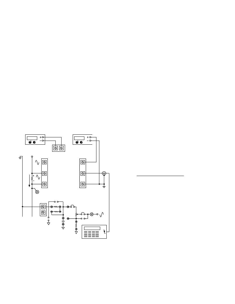
�Figure� 7� shows� a� wiring� diagram� that� allows� a� simple� energy�
�meter� to� be� implemented� using� the� AD7755� evaluation� board.�
�The� current� transducer� used� in� this� example� is� a� shunt� (400� μ?� ).�
�The� meter� is� intended� to� be� used� with� a� line� voltage� of� 220� V�
�and� a� maximum� current� of� 25� A.� The� frequency� outputs� F1� and�
�F2� can� be� used� to� drive� a� mechanical� counter.� These� outputs�
�will� be� calibrated� to� provide� 100� imp/kWhr.� The� logic� output�
�CF� has� an� output� frequency� that� can� be� up� to� 128� times� higher�
�than� the� frequency� on� F1� and� F2.� This� output� can� be� used� for�
�calibration� purposes� and� is� shown� connected� to� a� frequency�
�counter� via� the� optoisolator� in� Figure� 7.�
�At� maximum� current� (25� A),� the� power� seen� by� the� meter� will�
�be� 5.5� kW.� This� will� produce� a� frequency� of� 0.153� Hz� on� F1�
�and� F2� when� these� outputs� are� calibrated� to� 100imp/kWhr�
�(100imp/hr� =� 0.02777� Hz,� 0.02777� � 5.5� =� 0.153� Hz).� From�
�Table� III� in� the� AD7755� data� sheet,� the� closest� frequency� to�
�0.153� Hz� in� the� half-scale� ac� inputs� column� is� for� F� 2� ,� i.e.,� 0.17� Hz.�
�Therefore� F� 2� is� selected� by� setting� S0� =� 1� and� S1� =� 0.� The�
�choice� of� CF� frequencies� in� this� mode� (see� Table� IV� in� the�
�AD7755� data� sheet)� are� 32� times� F1� and� 64� times� F1.� For� this�
�example� 64� times� F1� is� selected� by� setting� SCF� =� 1.�
�Since� the� voltage� on� Channel� 1� is� fixed,� the� only� possible� way� of�
�calibrating� (adjusting)� the� output� frequency� in� F1� and� F2� is� by�
�5.000V�
�SK3B�
�SK3A�
�5.000V�
�JP20� =� CLOSED�
�varying� the� voltage� on� Channel� 2.� This� is� carried� out� by� varying�
�the� attenuation� of� the� line� voltage� using� the� trim� pot.�
�First� we� can� calculate� the� voltage� required� in� Channel� 2� in� order�
�NEUTRAL� PHASE�
�AGND� AVDD�
�JP21� =� CLOSED�
�to� calibrate� the� frequency� on� the� logic� outputs� F1� and� F2� to�
�100imp/kWhr.� The� AD7755� data� sheet� gives� the� equation� which�
�8� .� 06� � V� 1� � V� 2� � Gain� � F� 1� ?� 4�
�Freq� =� (1)�
�220V�
�SHUNT�
�5A�
�SK2B�
�2mV�
�SK2C�
�TP11�
�AGND�
�V1N�
�V1P�
�JP1� =� OPEN�
�JP2� =� CLOSED�
�JP3� =� OPEN�
�JP4� =� OPEN�
�JP5� =� OPEN�
�JP6� =� OPEN�
�JP12� =� B�
�JP19A� =� CLOSED�
�JP22� =� CLOSED�
�SK5A�
�6400�
�imp/kWhr�
�SK5B�
�SK5C�
�JP14� =� A�
�JP15� =� B�
�relates� the� voltage� on� Channel� 1� and� Channel� 2� to� the� output�
�frequency� on� F1� and� F2.�
�2�
�V� REF�
�First� a� current� is� selected� for� calibration,� 5� A� for� example.� This�
�gives� a� Channel� 1� voltage� of� 400� μ?� ×� 5� A� =� 2� mV� rms.� The�
�gain� of� Channel� 1� on� the� AD7755� is� set� to� 16� (G0� =� G1� =� 1).�
�JP7�
�JP16� =� A�
�JP17� =� A�
�The� on-chip� or� external� reference� of� 2.5� V� is� selected� using�
�SK1A�
�R53�
�JP52�
�JP18� =� A�
�JP13.�
�SK1B�
�LOAD�
�JP7� =� OPEN�
�JP8� =� OPEN�
�JP9� =� OPEN�
�R54�
�JP8�
�C53�
�JP50� =� P�
�JP51A� =� CLOSED�
�R55�
�R31�
�R56�
�A�
�B�
�JP51�
�218mV�
�V2P�
�1.9555� Hz�
�The� output� frequency� at� 5� A� on� F1� and� F2� should� be� 0.02777� Hz�
�(100imp/kWhr)� � 1.1� (220� V� � 5� A� =� 1.1� kW)� =� 0.03055� Hz.�
�From� Equation� 1� the� voltage� on� Channel� 2� should� be� set� to�
�218� mV.� The� attenuation� network� as� shown� in� Figure� 1� is� used�
�to� attenuate� 220� V� to� 218� mV.� R53� =� 660� k� ?� ,� R54� =� 100� k� ?� ,�
�R56� =� 500� ?� and� the� trim� pot� R31� =� 500� ?� .�
�JP10� =� CLOSED�
�JP11� =� N�
�JP52� =� CLOSED�
�R55� =� REMOVED�
�However,� since� the� meter� is� being� calibrated� at� CF� and� CF� is�
�Figure� 7.� AD7755� Evaluation� Board� as� an� Energy� Meter�
�–4� –�
�set� to� 64� times� F1,� the� voltage� on� Channel� 2� should� be� adjusted�
�until� CF� =� 64� � 0.03055� Hz� =� 1.9555� Hz� is� registered� on� the�
�frequency� counter.� The� counter� should� be� set� up� to� display� the�
�average� of� ten� frequency� measurements� on� CF.� This� will�
�remove� any� ripple� due� to� the� instantaneous� power� signal.� See�
�the� AD7755� data� sheet� for� more� details.�
�REV.� 0�
�发布紧急采购,3分钟左右您将得到回复。
相关PDF资料
EVAL-ADE7758ZEB
BOARD EVAL FOR AD7758
EVAL-ADE7759EBZ
BOARD EVALUATION FOR ADE7759
EVAL-ADE7762EBZ
BOARD EVALUATION FOR ADE7762
EVAL-ADE7763ZEB
BOARD EVALUATION FOR ADE7763
EVAL-ADE7816EBZ
BOARD EVALUATION FOR ADE7816
EVAL-ADE7878EBZ
BOARD EVAL FOR ADE7878
EVAL-ADE7880EBZ
BOARD EVAL FOR ADE7880
EVAL-ADE7953EBZ
BOARD EVAL FOR ADE7953
相关代理商/技术参数
EVAL-ADE7756EB
制造商:Analog Devices 功能描述:EVAL BD DOCUMENTATION ADE7756 ENERGY METERING IC - Bulk 制造商:Rochester Electronics LLC 功能描述:
EVAL-ADE7757AEBZ
制造商:Analog Devices 功能描述:EVALUATION BOARDS - Bulk
EVAL-ADE7757EB
制造商:Analog Devices 功能描述:EVAL BOARD ENERGY METERINGW/PULSE OUTPUT - Bulk
EVAL-ADE7758ZEB
功能描述:BOARD EVAL FOR AD7758 RoHS:是 类别:编程器,开发系统 >> 评估演示板和套件 系列:* 标准包装:1 系列:PSoC® 主要目的:电源管理,热管理 嵌入式:- 已用 IC / 零件:- 主要属性:- 次要属性:- 已供物品:板,CD,电源
EVAL-ADE7759E
制造商:AD 制造商全称:Analog Devices 功能描述:Active Energy Metering IC with di/dt Sensor Interface
EVAL-ADE7759EB
制造商:Analog Devices 功能描述:Power Metering, Active Energy Metering IC with di/dt Sensor Interface 制造商:Analog Devices 功能描述:EVAL FOR EN METER IC W DI/DT SENS INTRFC - Bulk
EVAL-ADE7759EBZ
功能描述:BOARD EVALUATION FOR ADE7759 RoHS:是 类别:编程器,开发系统 >> 评估演示板和套件 系列:- 标准包装:1 系列:- 主要目的:电信,线路接口单元(LIU) 嵌入式:- 已用 IC / 零件:IDT82V2081 主要属性:T1/J1/E1 LIU 次要属性:- 已供物品:板,电源,线缆,CD 其它名称:82EBV2081
EVAL-ADE7762EBZ
功能描述:BOARD EVALUATION FOR ADE7762 RoHS:是 类别:编程器,开发系统 >> 评估演示板和套件 系列:- 标准包装:1 系列:- 主要目的:电信,线路接口单元(LIU) 嵌入式:- 已用 IC / 零件:IDT82V2081 主要属性:T1/J1/E1 LIU 次要属性:- 已供物品:板,电源,线缆,CD 其它名称:82EBV2081